Common Data : VDD = 1.8V , Lmin = 0.18µm, µ0N = 350cm2/V s, µ0P = 100cm2/V s,
|VTH | = 0.55, tox = 3.8nm, λ = 0.07V−1, χ = 0.1.
1. For a MOSFET operating in the linear (triode) region (ignore body effect and channel- length modulation), find an expression for:
- the small-signal transconductance gm
- the small-signal drain-source output resistance rout
Comment upon your findings. Is it desirable for an amplifier to work in the linear region? Explain.
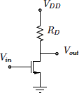
2. Consider the simple MOS amplifier shown in Figure 2. Assume λ = 0 and VDD = 1.8V.

Figure .2
Assume that the biasing for the gate side of the MOS is taken care of.
- For maximum symmetrical swing in Vout and for a drain current of 0.8 mA, find the required value of RD .
- Calculate the maximum symmetrical output swing, and also the small-signal volt- age gain in this case.
- How would the design values and the voltage gain change, if λ = 0.07 V−1?
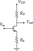
3. Consider the circuit in Figure 3.

Figure. 3 Circuit for Q3
If ID = 0.5mA, RD = 1.5kΩ and RS = 300Ω, calculate:
- the small-signal voltage gain
- the input voltage which will place the NMOS on the border of linear/saturation region, assuming γ = λ = 0. What would be voltage gain under this condition?
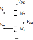
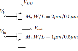
4.Consider the circuit shown in Figure 4. Assume VDD = 1.8V . The amplifier has to be designed such that ID = 100 µA.

Figure. 4 Circuit for Q4
- What should be the bias voltage Vb for the required ID ?
- What are the maximum and minimum values of Vout required to keep both M1 and M2 in saturation?
- Calculate the small-signal voltage gain offered by this circuit .
This problem is to be attempted similar to the problem 5 of the tutorial, i.e., by closing the cap and subtracting the contribution due to the cap. The divergence being 3, the flux from the closed cone is 3 times the volume of the cone which gives  The contribution from the top face (which is a disk of radius 2 ) is
  . Thus the net flux is zero. (You can also try to get this result directly as done in problem 4, where we showed that the flux from the curved surface is zero).
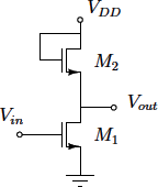
5. Consider the circuit shown in Figure 5.

Figure. 5 Circuit for Q5
- What are the maximum and minimum values of Vout required to keep both M1 and M2 in saturation?
- Obtain an expression for the small-signal voltage gain offered by this circuit.
6. Consider the circuit in Figure 6. Assume VDD = 1.8 V.

Figure. 6 Circuit for Q6
- What should be the bias voltage Vb if this amplifier is to provide a small-signal voltage gain of 25 ?
- What are the maximum and minimum values of Vout required to keep both M1 and M2 in saturation ?
- How would the voltage gain change if M2 were replaced by an ideal current source that provides the same current as required in part (a)?
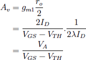
- Since M2 is a current-source load, it should be in saturation. Also, M1 should be in saturation. The small-signal gain of the circuit is thus given by

Since the λ of both transistors are equal, we have ro1 = ro2 = ro. Thus,

Substituting the values, we find, VGS − VTH = 0.57V. Thus, the current through M1 is approximately 0.2mA. The same current should flow through M2 as well. So we obtain the VGS for M2 to be approx. -1 V. Thus, Vb = VDD − VSG = 0.8 V.
-
For M2 to be in saturation, we need VDS < VGS − VTH , i.e Vout − VDD < −0.45 ⇒
Vout < 1.35 V. Thus, the maximum allowed Vout is 1.35 V. For M1 , we need Vout > VGS − VTH ⇒ Vout > 0.57V. Thus, the minimum allowed Vout is 0.57V.
-
An ideal current source would have an infinite resistance. Thus, there would be no ro2 as offered by M2. The gain expression would thus have reduced to Av = gmro, hence for the same current as in part (a), the gain would now be 25 × 2 = 50 .
![]() which gives
which gives ![]() Parameterize
Parameterize ![]() ,Since we are confined to the first octant
,Since we are confined to the first octant ![]() The flux through the slant surface is
The flux through the slant surface is ![]() . The top and the bottom caps are in the
. The top and the bottom caps are in the ![]() directions, the contribution from these two give zero by symmetry. There are two more surfaces if we consider the first octant, they are the positive x-z plane and the positive y-z plane., the normal to the former being in the direction of
directions, the contribution from these two give zero by symmetry. There are two more surfaces if we consider the first octant, they are the positive x-z plane and the positive y-z plane., the normal to the former being in the direction of ![]() while that for the latter is along
while that for the latter is along ![]() directions. The flux from the former is
directions. The flux from the former is ![]() , while that from the latter is
, while that from the latter is ![]() . Adding up all the contributions, the total flux from the closed surface is zero. This is consistent with the fact that the divergence of the field is zero.
. Adding up all the contributions, the total flux from the closed surface is zero. This is consistent with the fact that the divergence of the field is zero.